Industrial solutions

Precision inspection.
From wafer to package.

Explore semiconductor inspection equipment for optical defect detection, dimensional measurement and internal package analysis.

AOI Optical inspection3D MetrologyAXI X-ray inspection
Semiconductor equipment

Start with the defect.
Match the inspection.

Wafer fabrication and advanced packaging need different inspection approaches. Explore the equipment categories below, then share your samples, defect criteria and production requirements.

Technical information is based on TT Vision product information and the supplied brochures. Confirm the model configuration, availability and project requirements when you enquire.

Core products / Semiconductor packaging inspection

Two platforms.
From wafer to wirebond.

Explore TT Vision's F2X wafer inspection family and F241/F4X wirebond AOI platform, with product details from the supplied 2026 brochures.

CORE PRODUCT 01 / WIREBOND AOI
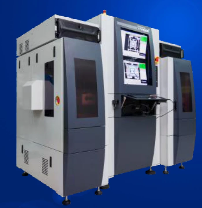
TT Vision F241/F4X wirebond AOI machine
TT Vision F241/F4X · Manufacturer brochure image

F241 / F4X

Wirebond AOI Machine

3D profiling for wirebond, die and epoxy defect inspection after bonding. Measure ball, wedge, stitch and loop parameters, including multi-stacked die and wires.

3D profilingMulti-stacked dieModular design
  • Inspect gold, aluminum, copper and silver wires
  • Conveyor or gripper handling; load/offload up to 3 magazines
  • Brightfield and darkfield illumination; all-image or defect-image saving
  • E-mapping reject handling and TCP/IP communication
F241/F4X · Published 2D vision options
MagnificationResolutionListed rate
1X3.45 µm/pixel80 SPH
1.5X2.3 µm/pixel40 SPH
2X1.72 µm/pixel20 SPH

Substrate range: 25 × 150 × 0.125 mm to 120 × 300 × 1.5 mm. Machine dimensions: 1500 W × 1200 D × 1800 H mm; weight: 900 kg. Rates are brochure values and depend on the selected inspection configuration.
CORE PRODUCT 02 / WAFER AOI
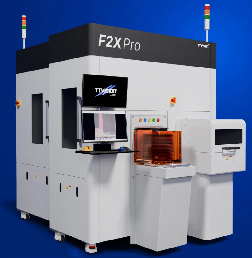
TT Vision F2X Pro wafer AOI machine
TT Vision F2X Pro · Manufacturer brochure image

F2X Series

Wafer AOI & 3D Metrology

A wafer inspection family covering surface defects, probe marks, sawing and bump defects, with dedicated models for 3D bump metrology and subsurface micro-crack inspection.

8-inch & 12-inch formatsAI-assisted classificationSECS/GEM
  • Rule-based and AI-based dual gate detection algorithms
  • Multi-magnification inspection and multiple illumination channels
  • Vibration-isolated granite stage and intuitive review software
  • Dual-arm cleanroom robot; gripper transfer for mounted wafers
F2X · Select the inspection model
ModelInspection focus
F2X ProWafer & sawn wafer surface AOI
F2X Pro+2D surface inspection & 3D bump metrology
Bump height range: 5–250 µm
F2X S3iSubsurface micro-cracks on sawn wafers

Pro / Pro+: 2X, 5X and 10X surface inspection; listed rates of 60, 35 and 15 WPH respectively. S3i is dedicated to mounted wafers, including invisible, bottom, side and inner cracks. Model performance depends on inspection mode and configuration.

Core ProductsWafer & Sawn Wafer AOISubsurface Micro-Crack Inspection2D Inspection & 3D MetrologyAutomated X-Ray InspectionWirebond AOISubstrate Package AOI
01 / WAFER INSPECTION

Wafer & Sawn Wafer AOI

Optical inspection of whole wafers and diced wafers, with attention to surface defects, probe marks, saw lines and bumps.

REFERENCE MODEL TT Vision · F2X Pro

Discuss your requirements

  • Wafer format and handling
  • Defect types and acceptance criteria
  • Required inspection coverage
02 / HIDDEN WAFER DEFECTS

Subsurface Micro-Crack Inspection

Optical inspection focused on internal micro-cracks in sawn silicon wafers before subsequent packaging stages.

REFERENCE MODEL TT Vision · F2X S3i

Discuss your requirements

  • Wafer material and doping
  • Target crack characteristics
  • Sample-based evaluation
03 / SURFACE QUALITY AND MEASUREMENT

2D Inspection & 3D Metrology

A combined approach to wafer surface-defect inspection and three-dimensional bump measurement.

REFERENCE MODEL TT Vision · F2X Pro+

Discuss your requirements

  • Surface-defect coverage
  • Bump-height measurement needs
  • Wafer and packaging configuration
04 / INTERNAL PACKAGE INSPECTION

Automated X-Ray Inspection

Non-destructive X-ray inspection for internal packaging defects, with configuration-dependent 2D imaging and optional 3D CT.

REFERENCE MODEL TT Vision · AXI X1

Discuss your requirements

  • Package structure and materials
  • Internal defects of interest
  • 2D or 3D inspection requirements
05 / POST-BOND INSPECTION

Wirebond AOI

Inspection of wirebond, die and epoxy features after bonding, including measurements of bond and loop characteristics.

REFERENCE MODEL TT Vision · F241 / F4X

Discuss your requirements

  • Wire materials and geometry
  • Bond and loop measurement needs
  • Handling and line integration
06 / PACKAGING QUALITY

Substrate Package AOI

Automated optical inspection of substrate surfaces using line-scan imaging, including top and bottom inspection.

REFERENCE MODEL TT Vision · F271

Discuss your requirements

  • Substrate dimensions
  • Surface defects and inspection criteria
  • Inline handling and reject workflow
VISION INSPECTIONILLUSTRATIVE WAFER INSPECTION CONCEPT
Application review

The right tool starts with the right questions.

Send the device or wafer format, target defects, throughput needs, handling method and factory interface requirements. Performance should be assessed against representative samples and the selected equipment configuration.

Prepare an equipment enquiry →

Let’s discuss your next project.

Share your application, drawings and technical requirements.

Discuss your project ↗